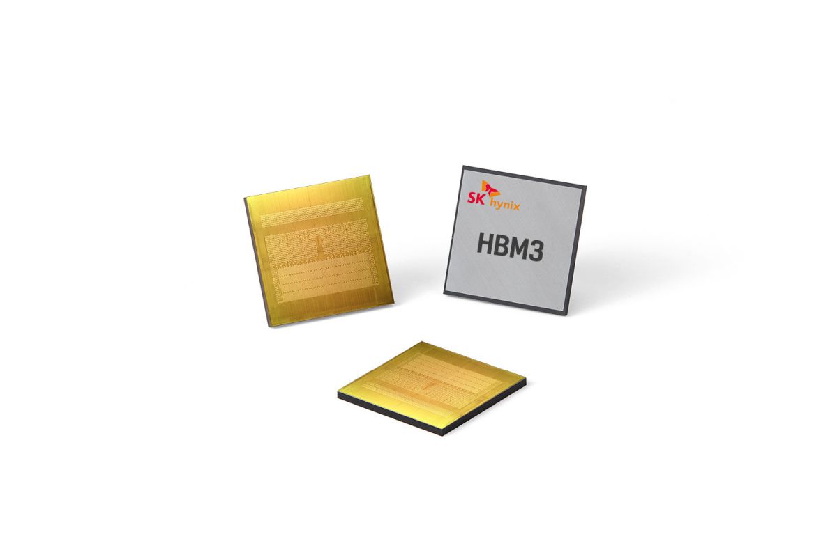
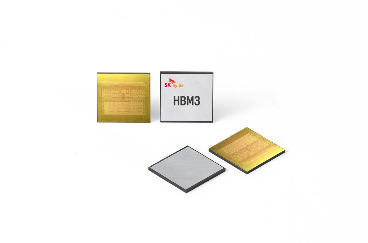
NVIDIA recently completed its performance review of HBM3 and did say during this year’s GTC event that it will be used in the company’s latest Tensor Core GPU, the H100. The GPU brand is expected to take order of the HBM3 chips for its HPC and accelerator systems, sometime in the beginning of the 3rd quarter of this year. So, not too far from now. In addition to the NVIDIA H100, it is also worth mentioning that it is the world’s largest and most powerful accelerator. The South-Korean company’s HBM3 is expected to boost accelerated computing speed by up to 819GB of memory bandwidth. For context, that is the equivalent of transmitting and playing 163 Full HD movies, at a 5GB standard size for each movie, per second. Additionally, Kevin (Jongwon) Noh, President and Chief Marketing Officer (CMO) of SK hynix, said that the corporation’s tight collaboration with NVIDIA has aided it in becoming and achieving top-tier competition in the premium DRAM market. It has been almost six years since the development and release of the HBM2. SK hynix says that with HBM3, it gets better as its new and improved DRAM comes with a much larger capacity, as well as a much higher level of quality. Due to this major upgrade, it is expected for the product to be utilised in the usual fare of HPC systems, including data centres and machine learning platforms. Considering the speedy advancements in cutting-edge technologies like artificial intelligence (AI) and big data, it is only natural and quite evident, as of this announcement, for major global tech organizations to look for ways to quickly process masses of data that are constantly increasing in a rapid fashion. To that end, we can’t wait to see the results HBM3 will bring to the table. (Source: SK hynix, Korea JoongAng Daily) Irfan Iskandar contributed to this article.

