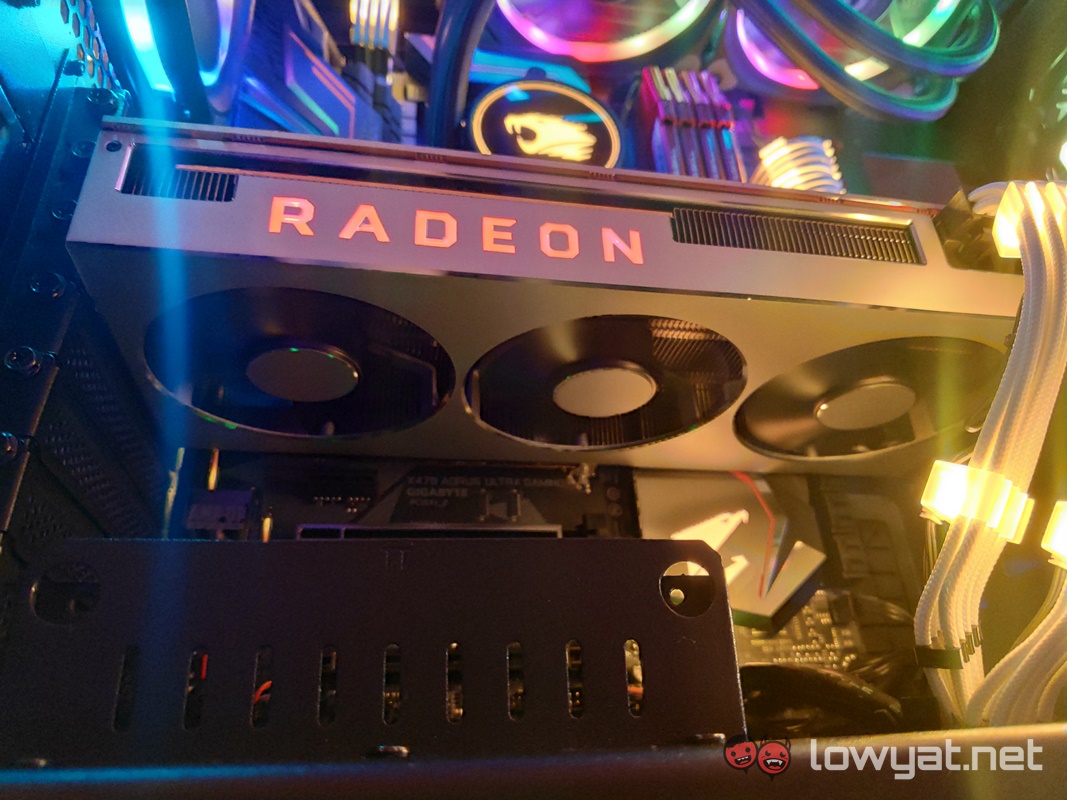
As per SK Hynix’s official post, its HBM2E memory is capable of a whopping 460GB/s that is, in turn, based on a 3.6Gbps per pin with 1024 I/Os. For context, that is an approximate 50% jump over the current generation HBM2. In addition, the memory can also be vertically stacked by a maximum of eight 16-gigabit chips at a time. Forming a single, dense package of 16GB capacity. Just as it had intended since the creation of the 1st generation of High Bandwidth Memory (HBM), SK Hynix is aiming for HBM2E to be utilised in high-performance GPUs. Dedicated to precision and mission sensitive assignments, including machine learning, deep learning, and supercomputing, to name a few. On another note, it is unlikely that HBM2E will ever grace a consumer card now or in the future. As it stands, GPU brand NVIDIA only uses the memory format for its Tesla and DGX supercomputers, and AMD has all but abandoned the memory standard for the more consumer-friendly GDDR6 memory format for its Radeon RX 5700 series GPUs. As for when HBM2E will be available, SK Hynix says that it intends to put the new memory standard into mass production by 2020, stating that that will be the year the “HBM2E market is expected to open up”. (Source: SK Hynix via Hot Hardware)
